DIY Game Boy Flash Cartridge with a ROM Adapter Board
Technical wiki guide for building a Game Boy flash cartridge using a ROM adapter board and compatible donor cartridge PCB.
Adapter-based flash cartridge build
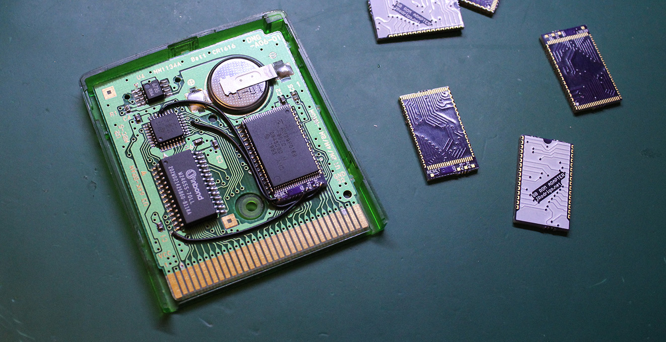
The idea is to reuse an original Game Boy cartridge PCB that already has a compatible mapper and footprint. After desoldering the read-only mask ROM, the adapter board is soldered where the original ROM was installed. Then a small number of extra signals are wired manually.
For a 2 MB flash ROM adapter, the practical wiring is normally three extra signals: RESET, RW and A20. For a 4 MB flash ROM adapter, add A21.
This adapter is only for 32-pin SOP parallel ROM footprints. Before soldering anything, verify that the donor cartridge ROM footprint and pinout match the adapter board.
Known compatible donor PCB families
Compatible cartridge PCBs include several MBC5, MBC3 and MBC7 mapper families. Other cartridges can also be compatible if the cartridge ROM footprint matches the adapter board and uses the same ROM pinout.
Treat this table as a starting point, not a complete compatibility database. The donor board must be inspected before using it: mapper type, ROM footprint, RAM support and battery requirements all matter.
Confirm the 32-pin SOP ROM footprint
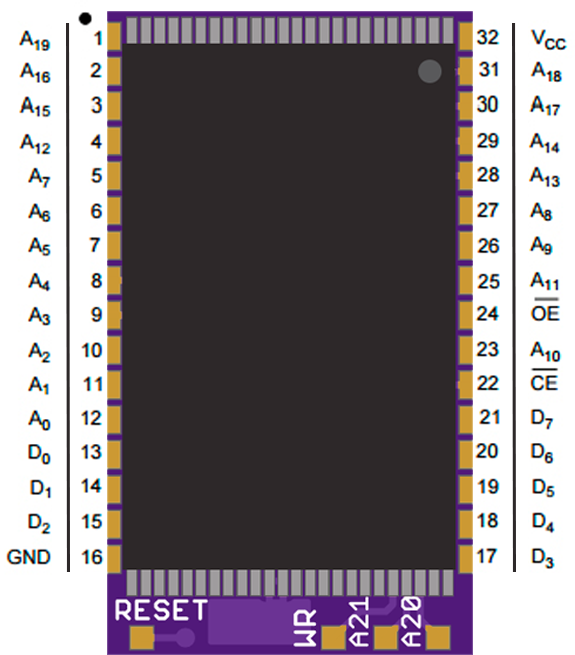
The adapter board is designed around a parallel ROM-style pinout. The donor cartridge must expose the right mask ROM footprint so the adapter can replace the original read-only ROM without rewiring every address and data line manually.
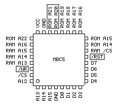
Reset/control signal. On MBC5 boards this may be marked as /RST.
Write control signal. On MBC5 boards this may be marked as /WR.
Extra address line used by larger flash ROM capacities.
Only needed for the 4 MB adapter variant.
Adapter board reference
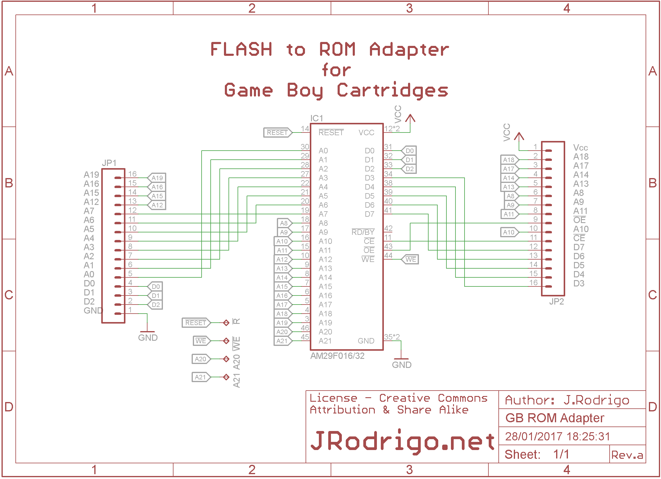
The schematic documents how the flash ROM adapter maps onto the cartridge ROM footprint. Use it as the reference when checking continuity, signal names and any mismatch between donor cartridge and adapter board.
Desolder the mask ROM, install the adapter, wire the extras
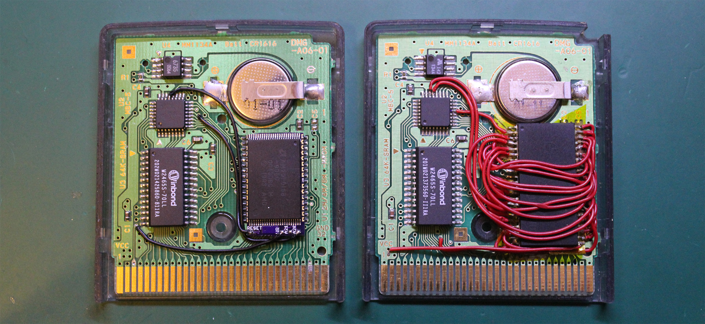
Remove the original mask ROM
Desolder the read-only ROM from the donor cartridge carefully. It is normally marked as U1 2M/4M/8M-MROM and is usually located below the backup battery on compatible boards.
Clean the footprint
Clean the remaining solder before installing the adapter. Flux and copper braid make the next soldering step much safer and reduce the chance of bridges between SOP pads.
Solder the ROM adapter board
Place the adapter in the old ROM footprint and solder it as the ROM replacement. Check alignment before committing all pins.
Wire the required signals
Add the extra wires for RESET, RW, A20 and, only for 4 MB adapters, A21. The wires can be soldered directly to the mapper IC or to a via/trace carrying the same signal.
Erase first, then program as a flash cartridge
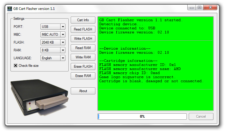
The first time the cartridge is programmed, erase the flash memory first. Use the Erase Flash button before writing a ROM.
After erasing, program it like other supported flash cartridges: choose MBC AUTO, select the appropriate flash/ROM size, and set the RAM size according to the donor board.
Useful external references
These links are useful when identifying donor boards and checking PCB variants.